Lab 2: Multiplexed 7-Segment Display
Introduction
This lab aimed to gain familiarity with clock multiplexing and PNP transistors, through driving 2 seven segment displays with a single set of GPIO pins that rapidly switches back and forth at the same frequency as the power driving both displays. This gives the illusion that both are on simultaenously because our eyes cannot detect how fast the displays are switching on and off.
Design and Testing Methodology
This challenge of this lab was using a single seven segment display module, and a corresponding single set of 7 GPIO pins to control two different seven segment display panels with different numbers. The trick is to rapidly switch the signals on outputed by the pins, and at the same frequency change which display gets power. That gives the illusion that both segements are continuously illuminated, but in reality it is only ever one at a time. This requires some testing to make sure that all the parts work together as intended.
Seven Segment display
The display module takes a 4 bit signal and decodes it to control the seven segment display, ensuring that all digits were unique (ex: 6 and b must be distinguishable). The first step was to map each hexadeciaml digit to the seven segment display and determine which panels should be on. Then, this was implemented using a case statement in SystemVerilog which turned the truth table into hardware. This module was already tested in lab 1, and comfirmed with a testbench, so we can be sure that this module works as expected.
Clock divider
Likewise, the clock divider was used in lab 1 as well. The parameter that changes the TOGGLE_COUNT was modified to output a faster frequency than lab 1 so that the human eye cannot detect flickering, but it is otherwise unchagned. Again this has it’s own testbench to ensure proper functionality, but we can also use this knowing that it works correctly.
Top Level module
Simulating the top level module was probably the most challenging aspect of all of lab 2. I changed the TOGGLE_COUNT parameter to flip every cycle (halving the clock frequency), so that the wave forms were more managable. Next, the challenge was getting testvector coverage for all \(2^8\) combinations of input switches, and also ensuring that the control signals that turn each one on or off were lined up correctly. To do this, I wrote a python script that generated these test vectors so they didn’t have to be hand written. This made it very easy to modify the testvectors as I identified bugs and changed the functionality of the module (it took me a few iterations to get the top level module outputs correct).
This module also tests the mux and adder logic, and this is built into the testvectors.
Eye test
For this type of project, the simple eye test is very important. Just because the verilog works as expected, we need to make sure that the chosen frequency for switching digits is fast enough to not notice flickering, but slow enough to not see any digits bleeding into each other.
Technical Documentation:
The code for my project can be found on my github page. Lab2 Github Repository
Block Diagram
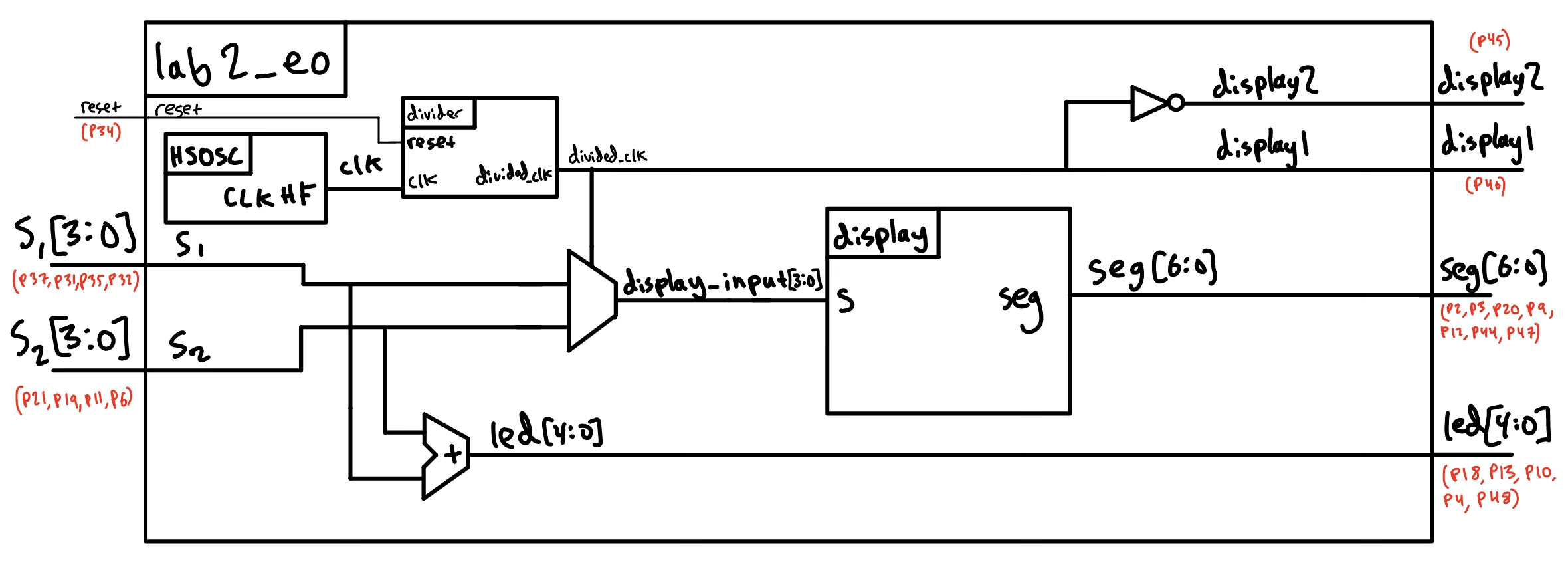
The block diagram in Figure 1 demonstrates the overall architecture of the design. The top-level module top includes three submodules: the high-speed oscillator block (HSOSC), the clock divider module (divider), and the seven segment display decoder (display).
It also includes a mux to switch between the two DIP switch input signals, an adder to sum together the input signals, and an inverter to create a set of opposing display control signals (when one is one the other is off and vice versa).
Schematic
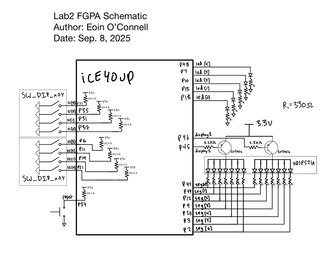
Figure 2 shows the physical layout of the design. We have 5 leds on the breadboard controlled by led[4:0], and these have current limiting resistors. The green LEDs that I am using have a voltage drop around 2.2 volts, so the current through the resistor is \(V/R = (3.3 - 2) / 330 = 3.9\) mA. This is an acceptable current for the FGPA pins. I used 1k \(\Omega\) resistors in lab1 and the LEDs were quite dim so I wanted to to have a brighter LED that was still safe for the FGPA in lab 2.
Additionally, I need resistors for the 7 segment display. In lab 1 I had current limiting resistors, but they were wired incorrectly and were not functioning as intended. Here I fixed that issue, but the calculation is the same from lab 1. The seven segment display has a typical forward voltage of 1.95 V (from datasheet), the PNP transistor has a Collector−Emitter Saturation Voltage of around 0.2 V, and given the 3.3 V input, we have an base voltage of \(3.3 - 1.95 - 0.2 = 1.15\). we get \(I = V/R = 1.15 / 330 = 3.48\) mA. This is an acceptable current for the FPGA GPIO pins, and the seven segment display has a bright clear ouptut, so this is what was used.
Finally, I need to calculate the resistor for the gate of the PNP transistor. From the data sheet, the Base−Emitter Saturation Voltage has a typical value of \(0.9\) V. That means the base is sitting at \(3.3-0.9 = 2.4\) V. My initial choice was a 2.2 k \(\Omega\) resistor, which gives \(2.4/2200 = 1.09\) mA through the FPGA pin. This is a perfectly acceptable FPGA current, and the transistor is operating correctly so it is used for this lab.
Results and Discussion
I accomplished all of the perscribed tasks: the 5 standalone LEDs display the sum of the two hexadecimal digits as expected, and the two digit seven segement display shows both digits with no flickering, with all digits at an even brightness. This is controlled by the 4 dip switches on the board, as well as a secondary set of dip switches on the breadboard.
Testbench Simulation
The first testbench is to simulate the top level module. We can see the waveforms match the expected values. For this test, I modified the parameter TOGGLE_COUNT for the divider to make the divided clock only half the frequency of the regular clock. This allows for a much more managable testbench as we do not need to wait thousands of cycles for the divided_clk to flip.
To generate the long test vectors file for the top level module to have complete coverage of all input combinations, I wrote a short python script generate_lab2_eo_testvectors.py which loops through all input combinations and appends one cycle with the first digit illuminated, and a second cycle with the second digit, before moving to the next switch combination. This made it very easy to modify the test vectors as I developed the module itself, instead of working on a very large complex testvector file directly.
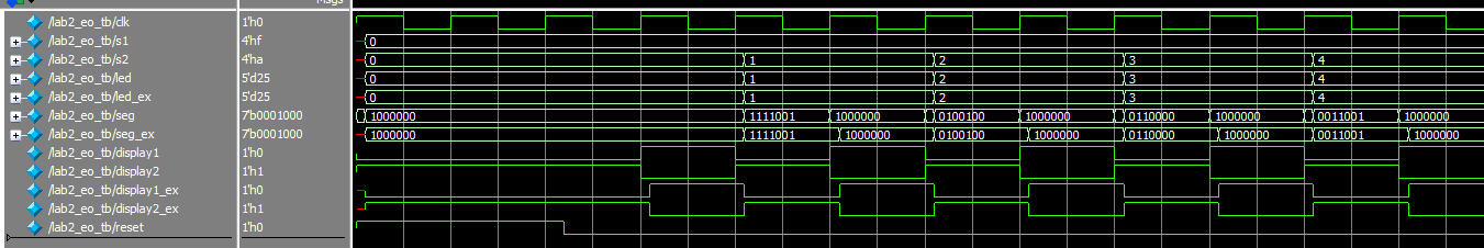
In figure 3, we see that the expected and simulated waveforms match. Of course, this is only the first couple cycles, but this continuous for all 512 tests. The 512 tests covers all \(2^8\) combinations of switches twice, as it includes 2 cycles per combination to allow the mux to select both inputs and flash the number on the respective panel.

Figure 4 output also confirms that the 512 tests matched the expectation, including the LEDs, the seven segment display, and the display selection signals.

Here, we are using the exact same unmodified display module from lab1, and we have the same test bench to confirm it’s functionality. We test for all combinations of s, and ensure that the 7 bit binary output is as expected.

Figure 6 shows that all 16 possible combinations of s matched the expectation.

Just like the seven segment display decoder, we are reusing the clock divider as well.
Here we can see that the test verison spends 10 cycles at zero and 10 cycles at one. This divides the frequency by 20. This testbench is much easier to keep track of then trying to simulate the clock divider counting thousands of cycles, yet still provides confirmation that it is working as intended.

Figure 8 gives confirmation that the module outputs match the expected values for all tests.
Conclusion
I found lab 2 significantly easier than lab 1, because I had a gained familiarity with the software and board, and had already assembled my parts. The verilog itself was also very quick, as I was able to reuse my display and divider modules from lab 1. Therefore, I had the verilog and testbenches written in around 2 hours.
It took around 2 more hours to assemble my breadboard, and 2 hours debugging some subtle issues. One such issue was that my verilog assumed a active high reset, wheras the board button is active low. That caused the digit to be stuck on one of them and not oscillate back and forth.
Overall, I worked on this lab for around 12 hours including the writeup and diagrams.
The FPGA succesfully controlled both digits on the seven segment display with no noticable flickering, and the 5 led lights that display the sum. The lab was very succesful and I enjoyed working on it.
I still had issues getting the FPGA programmer to help, but Javier gave me a useful tip which seems to be helping. I might still try out the alternative programmer that has been suggested.
AI Prototype Summary
Prompt 1: Write SystemVerilog HDL to time multiplex a single seven segment decoder (that decodes from four bits to a common anode seven segment display) to decode two sets of input bits and drive two sets of seven output bits.
I used my ChatGPT free account to create this, and the file is here on my github.
I opened up the verilog in Radiant, it synthesized without any issues. The first thing I noticed when looking at the Netlist analyzer is that there are 2 sets of seven segment display outputs. I think that the wording of the prompt suggests this, and that if I wanted to run this on my board (which doesn’t have enough GPIO pins to allow 14 pins for the seven segment display) I could easily ask Chat to fix this for me. Essentially, I think that it was correct for what it was trying to do.
Looking at the SystemVerilog itself, I noticed that while the AI included pleanty inline comments explaining what each line does, the over style was very poor, with no modules. I think that by modifying the prompt to tell it to use a modular design it would do well on this.
Next I tried the second prompt given in the lab manual.
Prompt 2: Write SystemVerilog HDL to time multiplex a single seven segment decoder (that decodes from four bits to a common anode seven segment display) to decode two sets of input bits and drive two sets of seven output bits. Use the seven segment decoder and oscillator provided in the attached files.
For some reason, despite providing the files as context, the LLM did not use the correct port names when instantiating the modules. For example for the divider it used clk_in and clk_out instead of clk and divided_clk which my module uses. Likewise it used in and out for the seven segment display instead of s and seg. It also got the parameter name TOGGLE_COUNT wrong and called it n. Somehow it new what the inputs, outputs, and parameters were, but somehow did not copy over the names correctly.
I performed those manual changes, the design synthesized correctly. It got the oscillator correct, and the rest of the SystemVerilog code seems reasonable (but also not modular like Prompt 1 response).
I think that a lot of these errors would be better with a different model and IDE such as Cursor instead of providing the files to chat gpt. During my internship I found that Cursor + Claude Sonnet worked very well and didn’t make these kinds of mistakes, but I do not have access to these anymore. For things like writting modular code, style, and comments, something like a Cursor rules file, or a thing that you add to every prompt/conversation with specific instructions would help get results that are closer to what the user desires.