Project Proposal: Real Time 3-Band EQ Filtering
Project Proposal
Overview
We will create a real-time 3-band equalizer (EQ) that can independently remove or boost lows, mids, and highs in an incoming audio signal. The system will feature three control knobs, one for each frequency range.
The project will accept audio through a standard 1/8-inch (3.5 mm) auxiliary input, allowing playback from a computer or mobile device. The analog audio signal will be digitized by an ADC, processed in real time by an FPGA using digital filtering, and then converted back to analog via a DAC for playback through a pair of speakers (left and right).
The design is going to be developed and implemented on an STM32L432KC Microcontroller, and an iCE40 UltraPlus FPGA.
Functional Specifications
-
- Low band: ~100 Hz – 400 Hz
- Mid band: ~400 Hz – 2 kHz
- High band: ~2 kHz – 8 kHz
- Low band: ~100 Hz – 400 Hz
System Partitioning
FPGA Responsibilities
- Perform real-time IIR-based filtering for the three EQ bands.
- Handle I²S communication with both ADC and DAC devices.
- Generate appropriate clock signals using internal oscillators (HSOSC or LFOSC).
MCU Responsibilities
- Read three analog potentiometer inputs (one per frequency band).
- Compute IIR filter coefficients based on knob positions.
- Transmit updated coefficients to the FPGA via SPI.
Analog to Digital Converter (ADC) Responsibilities
- Convert analog data to digital data
- Communicate over I2S protocol
Digital to Analog Converter (DAC) Responsibilities
- Convert digital data to analog data
- Communicate over I2S protocol
Risks for project
- End-to-end latency (ADC → FPGA processing → DAC) or buffering delays cause audible lag, clicking, or make the system unusable for live monitoring.
- Making the ADC, DAC, MCU and FPGA clocks not synchronized
- Increased quantization noise from using 16-bit data paths
- High-frequency content aliasing into the audio band if the ADC sample rate or analog filter are insufficient.
- Incorrect wiring between components
- Output clipping at high volume damaging speakers or hearing.
- Exceeding FPGA LUT’s, and more importantly, DSP slices
- Our FPGA Contains only 8 16x16 DSP slices, requiring clever pipelining and multiplexing to filter all signals in time
Hardware Components
| Component | Quantity | Function | Interface | Approx. Cost | Notes |
|---|---|---|---|---|---|
| Adafruit PCM5102 I²S DAC | 1 | Digital-to-Analog Converter | I²S | ~$6 | 16–32 bit, 8–384 kHz sampling, 3.3V logic, 2.1 V-rms output |
| PCM1808 ADC | 1 | Analog-to-Digital Converter | I²S | ~$6 | 24-bit, 8–96 kHz sampling, 3.3–5V supply |
| STX-3000 Audio Jack | 1 | Stereo audio input connector | Analog | ~$1 | 3.5 mm TRS jack, through-hole and breadboard compatible |
| 3362 1/4-inch Square Trimpot Potentiometers | 3 | User control for low, mid, and high bands | Analog | Stockroom | Reads by MCU ADC pins |
| ICE40 UltraPlus FPGA Board | 1 | Real-time DSP core | I²C, SPI | On Hand | Performs all filtering |
| STM32L432KC MCU Board | 1 | User interface and coefficient computation | SPI, ADC | On Hand | Communicates with FPGA |
| Miscellaneous Components | n/a | Op-amps, resistors, capacitors, wires | Analog | Stockroom | Used for signal conditioning, biasing, and connections |
Subtotal parts cost: ~$13 (excluding lab stock components).
Shipping and Taxes: ~$8
Total external parts cost: ~$21.
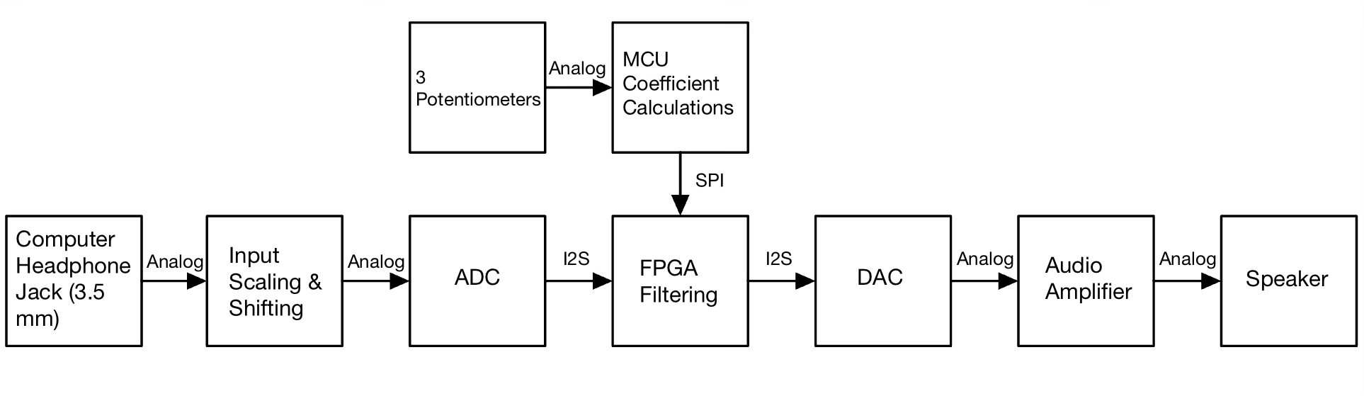
Block Diagram
Performance Calculations
The key performance characteristics of our EQ filter are defined by the sampling rate, ADC/DAC bit rate, and FPGA processing speed.
Sampling Rate / Nyquist:
By the Shannon–Nyquist theorem, the sampling frequency must exceed twice the highest signal frequency. Since the human ear can hear to around ~20 kHz, \(f_s > 40\,\text{kHz}\).
We will use 48 kHz, providing a 24 kHz Nyquist limit and headroom for filtering.
Bit Rate:
At 48 kHz, 24 bits/sample, and stereo audio:
\[ R = f_s \times B \times C = 48{,}000 \times 24 \times 2 \approx 2.3\,\text{Mbps} \]
With 32-bit I²S frames, the bit clock is approximately 3 MHz, easily handled by the FPGA.
FPGA Throughput and Latency:
Assuming a 48 kHz sample rate (sample period ≈ 20.83 µs), a 50 MHz fabric clock gives
\[ \frac{50\ \text{MHz}}{48\ \text{kHz}} \approx 1042 \]
cycles per sample, which is more than sufficient for three IIR filters using time-multiplexed multiplies. If the ADC and DAC run from the same sample clock and we complete filtering within one sample period, the per-sample processing latency is about 20.8 µs (\(\frac{1}{f_{ADC/DAC}}\)). The ADC/DAC and any pipelining typically add only a few samples of delay (on the order of tens of microseconds). Even with conservative buffering, end-to-end latency remains ≪ 50 ms, easily meeting our real-time requirement.
Resolution / Noise:
24-bit audio provides ~146 dB theoretical SNR; internal 32-bit accumulation will preserve precision and avoid quantization noise.
Overall, the design easily meets real-time performance needs: 48 kHz sample rate, <1 ms latency, and sufficient precision for transparent audio quality.
LUT Usage
Because the filtering is duplicated, we duplicate the filtering hardware. The 3-band EQ consists of 3 cascading filters (low, mid, high), with each band using biquads. That means that we do \(3 x 5 = 15\) multiplies per sample. These are 16 bit multiples, and the FPGA has 8 16x16 DSP slices. That means that as long as we run the FPGA at least 1.875 times the sampling frequency of the ADC/DAC then we can fit in all the multiplies. For a sampling rate of 48 KHz, this will be easy as the FGPA can run on order of MHz.
Project Timeline and Task Division
The table below outlines the major project milestones, their target completion dates, and the team member responsible for leading each task. Tasks are ordered chronologically to ensure smooth integration of the hardware and firmware components leading up to a functional prototype.
| Task | Goal Date | Lead Member |
|---|---|---|
| Order parts (after project approval) | As soon as approved | Drake |
| Successfully throughput unfiltered audio | 11/10 | Drake |
| Successfully demo filtering in MATLAB | 11/10 | Eoin |
| Successfully measure potentiometer input on MCU | 11/17 | Drake |
| Finish RTL design and verification via test benches | 11/17 | Eoin |
| Complete and test working prototype | 11/24 | Whole Team |
Task Division:
Drake will primarily focus on the hardware integration side of the project, including part procurement, audio signal interfacing, and MCU testing. Eoin will lead the digital signal processing implementation, including MATLAB filter validation and FPGA RTL design with test benches. Both team members will collaborate closely in the final integration and prototype testing phase to ensure seamless hardware–software coordination and successful real-time operation.
As the project progresses, we will monitor our progress and reallocate tasks as needed to ensure balanced workloads and timely completion. Work will be tracked through a shared action-items spreadsheet. Additionally, we both aim to maintain a complete understanding of the entire system, ensuring that each of us can independently explain and reproduce every part of the project.